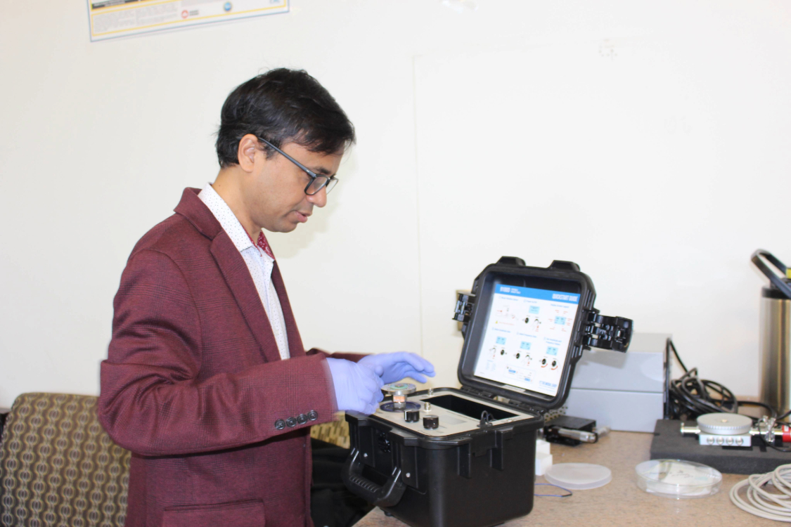
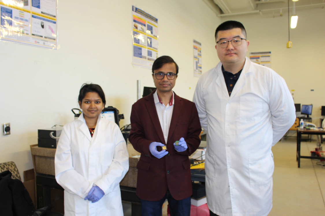
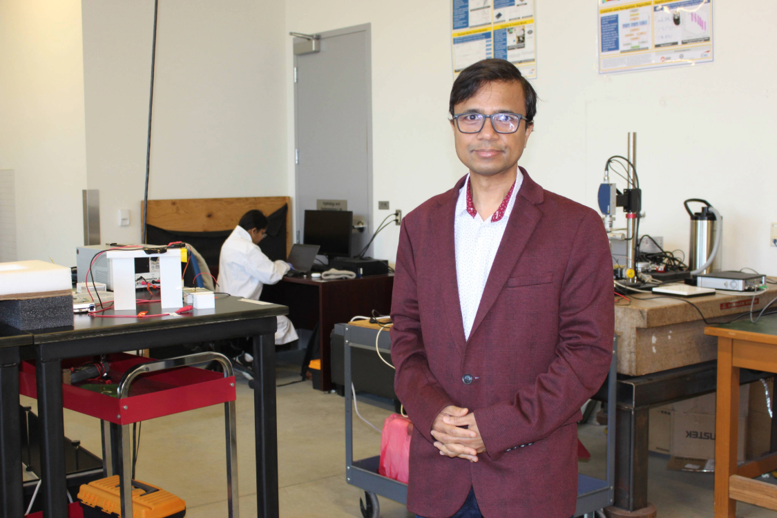
 Dr. Jalal Ahamed, mechanical, automotive and materials engineering professor, and lab manager Bhawya in the MicroNano Mechatronics Lab at the University of Windsor. (ANGELA KHARBOUTLI/ University of Windsor)
By Lindsay Charlton
Every time a car deploys an airbag, a smartphone tilts its screen or a satellite adjusts its position in space, tiny motion sensors are at work — quietly measuring movement with remarkable precision.
At the University of Windsor, researchers are working to push that technology further, developing next-generation sensors that are smaller, more accurate and better suited for large-scale manufacturing.
Dr. Jalal Ahamed, a professor of mechanical, automotive and materials engineering, has secured $1 million through the Natural Sciences and Engineering Research Council of Canada Alliance–Mitacs Accelerate program — $750,000 in cash and $250,000 in in-kind support — to develop nanoelectromechanical systems (NEMS), or nano chip-based motion sensors, for efficient, industry-ready production.
“These devices are widely used in many applications,” said Ahamed. “In vehicles, they’re used for stability, navigation, airbag deployment, environmental sensing and other safety systems.”
“They’re also applied in aerospace and robotics. Even everyday technology like smartphones, smartwatches and some video games rely on them to capture motion. Wherever there is a need to sense motion, these chips are applied.”
While silicon-based devices have long been the dominant technology, they do come with some limitations, Ahamed noted, particularly around stability, signal resolution, noise and long-term reliability.
The goal of the five-year project is to explore alternatives to create sensors that are more stable, sensitive, precise and smaller.
“At the moment, the devices are at the microscale, about the diameter of a strand of hair, roughly 100 microns,” he explained. “We’re already working at that level, but the goal is to make them even smaller, down to the nanoscale, which is about 1,000 times smaller in per unit scale.”
Another focus is developing the sensors in a cost-effective way to enable mass manufacturing. As Ahamed said, making NEMS at this scale is highly challenging and expensive, which limits wider adoption.
That’s where wafer-scale manufacturing comes in — a standard process in the semiconductor industry where many devices are made at once on a single silicon wafer before being cut into individual chips. The approach helps reduce production costs and enables large-scale manufacturing, Ahamed said.
“Through this project, we’re going to address those challenges,” he added. “What new physics will we encounter, and how can we overcome it? What are the limitations in manufacturing, and how do we overcome them so we can produce it at a larger scale?”
To do that, Ahamed and researchers in his MicroNano Mechatronics Lab will be working with industry partner Teledyne MEMS, a micro-electro-mechanical systems (MEMS) fabrication company based in Edmonton, Alta., that works with a range of high-tech companies.
"This NSERC–MITACS Alliance program enables Teledyne MEMS to directly advance wafer-level process technologies for next-generation MEMS and NEMS devices, including high-performance inertial sensors. By combining academic research from the University of Windsor with industrial fabrication expertise at Teledyne MEMS Edmonton, this collaboration accelerates the development of scalable and manufacturable sensor technologies,” Dean Spicer, director of engineering at Teledyne MEMS, said in a statement.
“This initiative builds on Canada’s expertise in advanced semiconductor manufacturing and contributes to the development of the highly skilled people needed to support our country’s high technology ecosystem.”
The Mitacs portion of the grant supports an internship at Teledyne MEMS, allowing five students each year the opportunity to work on research while gaining practical skills.
Mahir Chowdhury, a master’s student in mechanical engineering transitioning into a PhD, will be among those involved and said he is looking forward to the experience.
“This will involve designing, assembly, testing and characterization. I’ll be going to facility in Alberta to design and help fabricate the devices, since they have that capability there,” he said.
“Once fabricated, we’ll bring them back to our lab for testing. We have tools like a thermal control vacuum chamber, and we’ll also use lasers and probes to measure the response and compare it with what’s in the current literature.”
Chowdhury noted there is a lot of design and simulation involved to ensure the physics makes sense before reaching that stage.
“Those working on the project will eventually go to the facility, and what they do is send us to the clean room,” he said. “A clean room is a fabrication area where they create chips and devices, so we’d go in there, wear our bunny suit and try to keep the place super clean while we work on the chip.”
This is an important element, as Ahamed noted that a speck of dust is actually larger than many of the features in the centre chip.
He said the partnership allows the team to work on research and real-world application simultaneously.
“The students will be spending a good amount of time in industry. This is a unique opportunity for students to get their hands on industrial experience and collaboration while training them for emerging technology, for example, in semiconductors.”
Ahamed pointed to the global semiconductor shortage that disrupted multiple industries during the COVID-19 pandemic. Locally, the automotive industry was hit particularly hard, with plants regularly shut down for weeks in Windsor-Essex and across the country.
“We all learned the necessity of these microchips and the need for in-house manufacturing,” he said. “We are contributing to that again, making Canada-designed and manufactured devices to take this to a larger market.”
The federal government has made investments to further advance the industry in Canada, and as Ahamed pointed out, this will require people trained in that area.
“These are specialized skills which are not learned in conventional academic programs. But these students will receive that training,” he said.
“This is a five-year, large-scale project that will create opportunities for a significant number of students, with many graduate students and postdoctoral fellows trained for roles in the semiconductor industry.”
Demand for smaller, faster and more accurate sensors continues to grow across multiple sectors, Ahamed said.
“Everything is getting smarter, which means more of these sensing chips are needed across industries,” he said. “From vehicles and aerospace to consumer electronics and industrial systems.”